electronics circuit boards designs
When a product goes from concept to the store, there are a lot of moving parts. One small oversight can derail the whole process. One way to avoid these errors is to conduct Design for Manufacturability (DFM) on a circuit board before production begins. DFM checks ensure that the board will be fabricated successfully, avoiding costly revisions to the design.
In the PCB fabrication and assembly process, many different steps are involved. The fabricator first prepares the substrate, which is typically FR-4 and coated with a thin copper layer. Then, they verify design rule adherence and panelize designs for efficient manufacturing. Next, they create a photomask that represents the panelized design. After exposure and chemical washing, unwanted copper is etched away. Finally, a solder mask is applied to inhibit corrosion and aid assembly. Throughout the manufacturing process, electrical tests and automated inspections are performed to ensure consistency and quality.
To reduce the risk of electronics circuit boards problems, a good fabricator should have a vetted network of suppliers that use the same quality standards. This can significantly improve lead times and decrease the chance of counterfeit components making their way into a build. To further reduce the risk of quality issues, a reputable electronic manufacturer should be able to provide a full suite of testing and debugging services, which can help identify and resolve problems before they can impact functionality or performance.
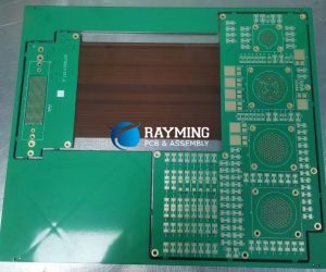
How do you ensure manufacturability in electronics circuit boards designs?
Using standard components is another way to reduce costs and speed up manufacturing times. Using non-standard components requires extra time and effort, resulting in longer lead times and higher costs. Standard components are also available in a wide range of options, which can help designers meet various application requirements without sacrificing manufacturability or cost.
Logical component placement can greatly ease the assembly process. This includes grouping similar components together and arranging them in an orthogonal pattern. This will allow for easier automation and routing and reduce the risk of solder bridges or other defects.
Another key to successful assembly is the correct component footprint size. Choosing the right size will help to prevent unnecessary assembly and routing steps, as well as reduce the chance of interference with other components. The smallest component footprints are usually used for the most critical components, such as high-speed signal traces and power traces. On the other hand, oversized footprints can be used for smaller components, such as passives and power resistors.
Finally, it’s important to consider thermal resistance and dissipation. The temperature of the PCB and its components can affect performance, so it’s a good idea to plan for heat sinks and cooling fans to minimize them. A quality PCB can make the difference between a great product and one that fails in the market. These simple tips will help you make a more efficient design, improving your chances of getting your product to market on time and within budget.