Back Drill a Standard Practice in PCB Manufacturing
PCB back drill, also known as controlled depth drilling, is an advanced feature that enables surgically reducing via stub length in multilayer printed circuit boards. It reduces signal loss and helps to achieve high-speed signal transmission. Its benefits include lowering signal distortion, improved impedance matching and EMI control. The additional benefit is higher routing density for high-speed digital and RF boards.
The main function of back drill is to remove the unused portion of a plated through hole (PTH) that doesn’t serve any connection or transmission functions, thereby avoiding issues such as reflection, scattering and delay in high-speed signal transmission. It is a very important process for high-speed electronic devices that require accurate and stable signal transmission. It is widely used in communication equipment, large-scale servers, medical electronics and military and aerospace applications.
To perform back drilling, a PTH must be drilled a specific amount larger than its original via or pad hole size. This “oversize” is specified as a radial amount in the back drill design rule along with any tolerance requirements for the back drilled holes. A typical oversize is 0.2mm larger than the original hole size, which ensures that the stub copper is removed.
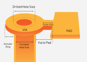
Is Back Drill a Standard Practice in PCB Manufacturing?
It is very important to clearly specify the drill size for a back drill in order to avoid drilling traces that shouldn’t be drilled. Additionally, it is critical to ensure that the back drill is bigger than the original hole in order to ensure that the copper plating on the back side of the PCB is removed, which is the purpose of the technique.
Using the back drill feature is easy in Eagle and is a good idea for all PCB designers. However, it is important to remember that the additional drilling step increases fabrication costs. It is therefore crucial to balance the necessary signal integrity performance with practical manufacturing considerations and constraints.
To generate a summary report of all back drill events in a PCB, right-click the Unique Holes region of the board panel in Hole Size Editor and select the Back Drill Report option. The report will display a list of all back drill locations on the board with the associated drill sizes and layer numbers.
The best PCB designs will utilize the back drill feature to eliminate unused stubs and improve signal quality, signal stability and EMI control. It is particularly important for high-speed digital and RF applications, as it significantly lowers jitter, timing errors and signal layer-to-layer crosstalk.
It’s also worth noting that back drilling does not reduce stub length on layers that don’t escape routing above the drilled area, such as blind or buried vias. For this reason, the technique is often employed in high-speed digital and RF PCBs that do not have viable blind or buried via options. Additionally, back drilling can be utilized to lower overall signal attenuation in high data rate signals and increase routing density on the board. This helps to reduce jitter, deterministic jitters and timing errors in a device’s internal logic circuitry.